群馬大学 理工学部 電子・機械類 知能制御プログラム
大学院理工学府 電子情報・数理教育領域

張 研究室
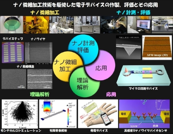
理論計算及びナノ微細加工技術を用いて超微細ナノ構造の形成、電子デバイスの作製及び計測に関する研究を行っています。
研究全体像と研究風景
全体像
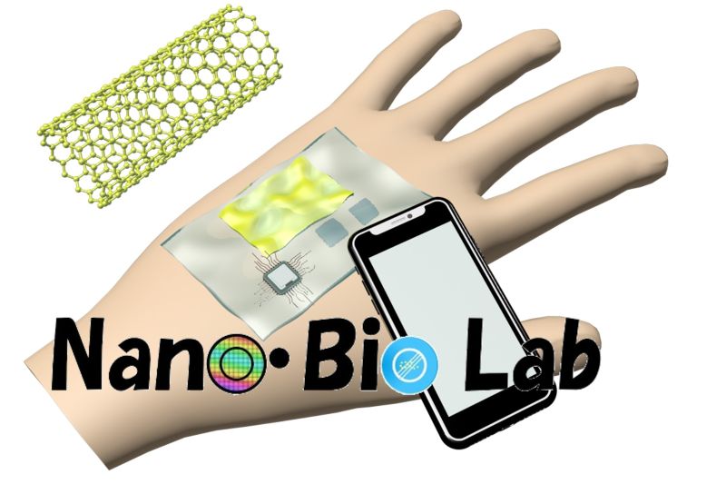
当研究室では、ナノ微細加工技術とバイオセンシング技術を融合させ、超高感度・迅速・多検体同時検出が可能なシリコンナノワイヤ(SiNW)バイオセンサの開発を進めています。
また、ナノ微細構造の形成やトライボエレクトリックナノジェネレータ(TENG)や電気化学バイオセンサ技術の応用にも取り組み、次世代の医療診断デバイスやエネルギーデバイスの創製を目指しています。
研究風景
※ 音声付きのため、再生時は音量にご注意ください(自動再生はしません)。
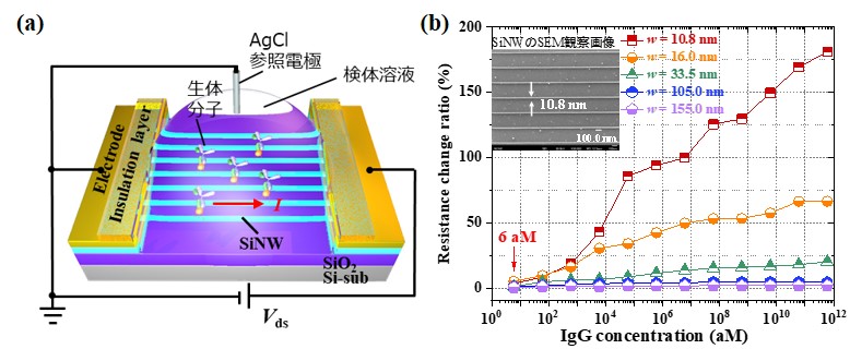
超高感度Siナノワイヤバイオセンサの研究
微量物質の検出技術は、医療やバイオ分野をはじめとする多様な分野で不可欠であり、特に化学物質や生体分子を簡便かつ高感度に検出する手法が求められています。
近年、その実現に向けて、電界効果トランジスタ(Field Effect Transistor: FET)の原理を応用したバイオセンサの研究開発が世界的に活発化しています。
FETバイオセンサの検出感度は、検出チャネルの構造および電界効果移動度に大きく依存します。
我々の研究グループでは、半導体プロセスによって形状や電気特性を精密に制御可能なSi材料に着目し、SiNWバイオセンサの研究を進めています。
SiNWの微細化と構造最適化により、サブ10 aM(1 aM = 10^-18 mol/L)という超低濃度検出に成功しています。
関連論文:
-
H. Zhang, F. Osawa, H. Okamoto, Y. Qiu, Z. Liu, N. Ohshima, T. Kajisa, T. Sakata, T. Izumi, and H. Sone,
“ Ultrasensitive Specific Detection of Anti-influenza A H1N1 Hemagglutinin Monoclonal Antibody Using Silicon Nanowire Field Effect Biosensors ”, ACS Appl. Bio Mater., Vol. 8, pp. 1038-1049 (2025).
H. Zhang, M. Abe, F. Osawa, Y. Qiu, N. Ohshima, T. Kajisa, T. Sakata, T. Izumi, and H. Sone,
“ “The possibility of ultrasensitive detection of biomolecules using silicon nanowire biosensor with structural optimization ”, Jpn. J. Appl. Phys., Vol. 63, pp. 03SP85 1-7 (2024).
H. Zhang, Y. Qiu, F. Osawa, M. Itabashi, N. Ohshima, T. Kajisa, T. Sakata, T. Izumi, and H. Sone,
“ Estimation of the Depletion Layer Thickness in Silicon Nanowire-Based Biosensors from Attomolar-Level Biomolecular Detection ”, ACS Appl. Mater. Interfaces, Vol. 15, pp. 19892-19903 (2023).
H. Zhang, N. Kikuchi, N. Ohshima, T. Kajisa, T. Sakata, T. Izumi, and H. Sone,
“ Design and Fabrication of Silicon Nanowire-Based Biosensor with Integration of Critical Factors: Toward Ultrasensitive Specific Detection of Biomolecules ”, ACS Appl. Mater. Interfaces, Vol. 12, pp. 51808-51819 (2020).
Tomoya Tashiro, Hui Zhang, Kakeru Oshima, Yuya Sakurai, Takaaki Suzuki, Noriyasu Ohshima, Takashi Izumi, and Hayato Sone,
“ Fabrication of N-type Silicon Nanowire Biosensor for Sub-10-Femtomolar Concentration of Immunoglobulin ”, Key Engineering Materials, Vol. 790, pp. 28-33 (2018).
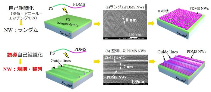
10 nm以下のナノ微細構造の形成
ドット径10 nm以下のドットパターンを形成するため、電子線描画法によるガイドパターンとブロック共重合体による自己組織化を組み合わせたナノドットパターン形成法を研究しています。
通常の自己組織化法では基板上にドットがランダムに形成されるが、精密に設計されたガイドランインパターンを用いて基板表面の領域を制限することで、世界最高水準となる直径5 nm、
ドット間隔10 nm×7.5 nmのドット列および幅10 nm以下のブロックコポリマーナノワイヤを形成しました。
関連論文:
-
Sumio Hosaka, Takashi Akahane, Kazumasa Ohyama, Hui Zhang, You Yin, and Hayato Sone,
“ Formation of 7-nm-wide Line & Spaces in Half Pitch by 3 Dimensional Self-assembly of Nano-dots Using Sphere Type PS-PDMS ”, European Journal of Applied Physics, Vol. 3(6), pp. 84-90, (2021).
Sumio Hosaka, Takashi Akahane, Miftakhul Huda, Takuya Komori, Hui Zhang, and You Yin,
“ Ordering of 6-nm-sized nanodot arrays with 10-nm-pitch using self-assembled block copolymers along electron beam-drawn guide-lines ”, Microelectronic Engineering, Vol. 123, pp. 54-57, (2014).
Zulfakri Mohamad, Miftakhul Huda, Takuya Komori, Rosalena Irma Alip, Hui Zhang, You Yin, and Sumio Hosaka,
“ Fabrication of 25-nm-Pitched CoPt Magnetic Dot Arrays Using 30-keV-Electron Beam Drawing, RIE and Ion-Milling ”, Advanced Micro-Device Engineering IV, Vol. 596, pp. 92-96, (2014).
Jing Liu, Miftakhul Huda, Zulfakri Bin Mohamad, Hui Zhang, You Yin, and Sumio Hosaka,
“ Fabrication of Carbon Nanodot Arrays with a Pitch of 20 nm for Pattern-Transfer of PDMS Self-Assembled Nanodots ”, Advanced Micro-Device Engineering IV, Vol. 596, pp. 88-91,(2014).
Sumio Hosaka, Takashi Akahane, Miftakhul Huda, Takuya Komori, Hui Zhang, and You Yin,
“ Fabrication of 6-nm-sized nanodot arrays with 12 nm-pitch along guide lines using both self-assembling and electron beam-drawing for 5 Tbit/in² magnetic recording ”, Advanced Micro-Device Engineering IV, Vol. 596, pp. 73-77, (2014年).
Sumio Hosaka, Takashi Akahane, Miftakhul Huda, Takuya Komori, Hui Zhang, and You Yin,
“ Ordering of 6-nm-sized nanodot arrays with 10-nm-pitch using self-assembled block copolymers along electron beam-drawn guide-lines ”, Microelectronic Engineering, Vol. 123, pp. 54-57, (2014).
Sumio Hosaka, Takashi Akahane, Miftakhul Huda, Hui Zhang, and You Yin,
“ Controlling of 6 nm Sized and 10 nm Pitched Dot Arrays Ordered along Narrow Guide Lines Using PS-PDMS Self-Assembly ”, ACS Applied Materials & Interfaces, Vol. 6(9), pp. 6208-6211,(2014).
Hui Zhang, Sumio Hosaka, and You Yin,
“ Ordering of self-assembled 5-nm-diameter poly(dimethylsiloxane) nanodots with sub-10 nm pitch using ultra-narrow electron-beam-drawn guide lines and three-dimensional control ”, Applied Physics Letters, Vol. 104(9), 093107, pp. 1-4, (2014).
摩擦ナノ発電デバイスの研究
近年、ウェアラブルデバイスの急速な普及に伴い、電源の小型化・軽量化・柔軟性が強く求められています。
摩擦帯電型発電デバイス(TENG)は、自律的に電力を供給できる点で注目されており、次世代電源への応用が大きく期待されています。
我々の研究グループでは、ナノ微細加工技術を活用して電極の微細化及びデバイス構造の最適化を図ることで、高出力密度を有するTENGデバイスの実現を目指しています。