Gunma University, Faculty of Science and Technology, Electronics and Mechanical Engineering, Intelligent Control Program
Graduate School of Science and Technology, Education Program in Electronics, Informatics and Mathematics
Zhang Laboratory
We use theoretical calculations and nanofabrication to form nanoscale structures and to fabricate and characterize electronic devices.
Research: Theoretical modeling and nanofabrication for electronic devices, their characterization, and applications in biosensing
“Nano” refers to fabricating nanostructures on silicon or silicon-on-insulator (SOI) substrates, characterizing them with nanoscale measurement techniques, and exploring their properties and applications. Nanotechnology underpins electronics, biotechnology, medicine, and environmental monitoring. It makes previously unattainable device and sensor performance possible and can help address challenges in these fields. Our work focuses on a small part of this broad discipline. As a young laboratory, we started with a focused research program and plan to broaden it gradually.
The “o” in “Nano” depicts integrated circuits on a silicon wafer.
“Bio” refers to using our electronic devices for biosensing. The COVID-19 pandemic highlighted the demand for tests that deliver results faster than PCR and offer greater accuracy than antigen–antibody tests. We develop biosensors for rapid, sensitive detection of trace biomolecules in samples. We fabricate silicon nanowires and use computational methods to study how sensor geometry, electrical properties, and surface conditions influence detection. Ultimately, we aim to develop a system that can measure multiple biomolecules simultaneously from a single clinical sample.
The “o” in “Bio” depicts a silicon nanowire sensor assembled with a reaction tube over the sensing area for measurements in solution.
Nanoelectronic devices use nanoscale structures or materials (1 nm = 10⁻⁹ m). Our silicon nanowire (SiNW) biosensor is a transistor in which a nanowire patterned in the top silicon layer of an SOI substrate serves as the channel between two electrodes. When target biomolecules bind to the functionalized nanowire surface, their charge interacts electrostatically with carriers in the wire through the thin insulator and depletion region. The resulting change in depletion width is detected as a change in current.
We perform the full fabrication process in-house, from doping the substrate to making the electrodes and nanowires and packaging the device.
Nanofabrication and Characterization
We fabricate nanostructures and electronic devices using electron-beam lithography, photolithography, sputtering, and reactive ion etching. We characterize the resulting structures using scanning electron microscopy, atomic force microscopy, stylus profilometry, and X-ray photoelectron spectroscopy (XPS). Low-current measurement instruments enable detailed electrical characterization. Combining these fabrication and measurement methods helps us evaluate nanoscale structures and develop advanced electronic devices.
Simulation
We use computational physics methods, including Monte Carlo simulation of electron transport, to guide nanostructure and device fabrication. For high-sensitivity SiNW biosensors, we use finite-element analysis to compare the relative changes in current and resistance before and after biomolecular binding across different nanowire geometries and predict suitable sensor designs.
Principal Investigator
Hui Zhang
Current appointments
Associate Professor, Intelligent Control Program, Electronics and Mechanical Engineering, Gunma University
Researcher, JST Fusion Oriented REsearch for disruptive Science and Technology (FOREST)
Visiting Researcher, Institute for Ambient Electronics, Waseda University
Degree
March 2013 — PhD in Engineering, Gunma University
Career
April 2013–March 2016 — Postdoctoral Researcher, Gunma University
October 2016–March 2017 — Research Associate, Nano & Life Innovation Research Organization, Waseda University
April 2017–March 2019 — JSPS Postdoctoral Fellow for Research in Japan
April 2019–March 2025 — Assistant Professor, Electronics and Information Division, Graduate School of Science and Technology, Gunma University
April 2025–present — Associate Professor, Intelligent Control Program, Electronics and Mechanical Engineering, Gunma University
新井 貴之 (M2, jointly supervised with Professor Hayato Sone)
梁 城強 (M2, jointly supervised with Professor Hayato Sone)
Fumiya Osawa (D3, jointly supervised with Professor Hayato Sone)
Yawei Qiu (D3, jointly supervised with Professor Hayato Sone)
Lab Activities
Weekly Research Meetings
We report on the week’s research, discuss experimental methods and problems, and often gain a better understanding of the principles behind our work. The meetings give us a chance to exchange ideas, share new approaches, and work together to move our projects forward.
English Seminar
We hold the English seminar after research progress presentations, except during busy periods, from April to June and October to December.
Activities include vocabulary and composition exercises, translation and discussion of research-related books, listening practice, and conversations on assigned or freely chosen topics. They help us improve our English and build knowledge relevant to our research. Let’s discuss!
Hands-On Nanofabrication Training
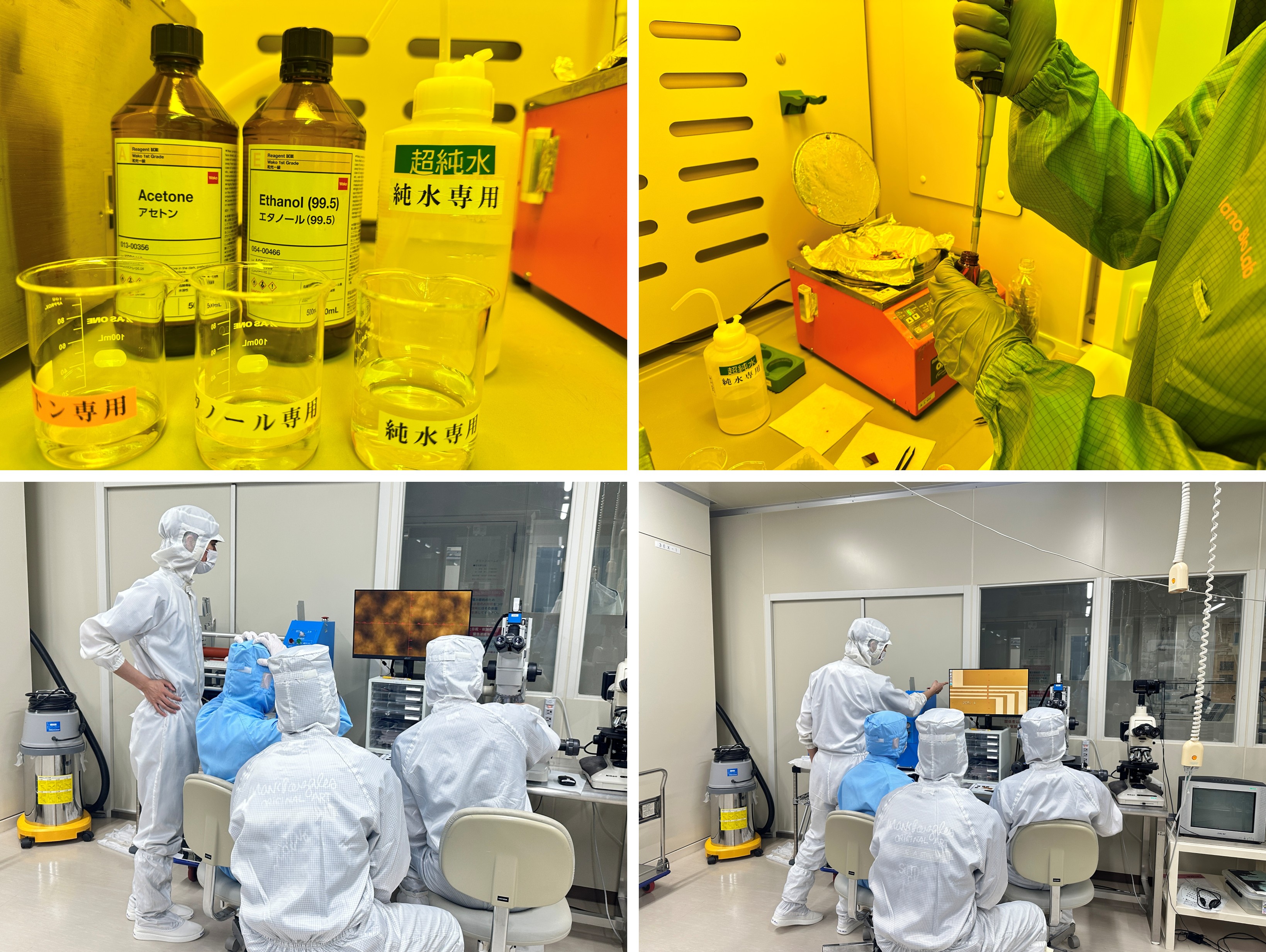
Fourth-year undergraduates joining the lab receive hands-on training in fabricating micro- and nanoscale structures and devices.
It is fine if some things are new to you at first. We cover equipment operation and process design from the basics, so you can experience how a fabricated structure becomes a working device.
Cherry Blossom Viewing
Lab members gather during cherry blossom season to enjoy the blossoms and spend time together. It is a chance to get to know one another in a relaxed setting away from our day-to-day research.
Social Gatherings
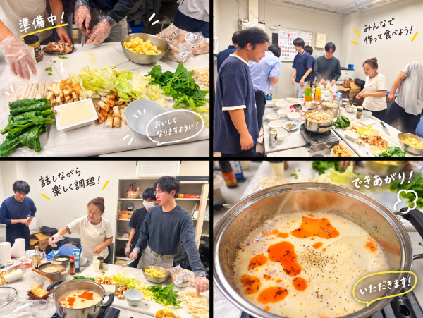
We get together from time to time, for example when new members join or after undergraduate and master’s thesis presentations. A lab member takes charge of organizing these gatherings. A dumpling cook-off or a barbecue might be next. We look forward to seeing what they plan.
Photo: Malatang party, August 2026→
Annual Lab Retreat
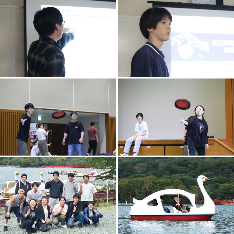
Every September we hold a two-day retreat at the National Akagi Youth Exchange Center, surrounded by nature. We discuss research progress and challenges, spend more time talking than we usually can in the lab, and share a meal in the evening. Afterward, there is time to explore Mount Akagi and try local food.
Photo: September 2026 lab retreat at Mount Akagi→
Conferences
We encourage lab members to present their results at domestic and international conferences. Presenting gives us a chance to learn from other researchers’ feedback and perspectives, and to develop communication and presentation skills for future research and careers. After the sessions, there may also be time to explore the area and try local food.
Photo: MNC 2025, Tokyo→
For more about these lab activities, see News & Photos.
Messages for Future Lab Members
A friendly lab where it’s easy to ask for help
Students in the lab get along well. When you’re unsure about something, you can ask a senior student or someone in your year. When an experiment doesn’t go as planned, you can talk it through with others and work out a solution together. Our supervisor is approachable, so you can discuss your plans and results and feel comfortable moving ahead with your research.
Senior student O
Try semiconductor processing yourself
Our supervisor and senior students know the equipment well and patiently show you how to use it. Turning a plain silicon substrate into something you designed is an incredible feeling of accomplishment and an experience you’ll always remember.
Senior student L
A place to take on challenges
The Zhang Lab gives you the people, environment, and equipment to try things without fear of failure. As the saying goes, failure is a stepping stone to success. Let’s learn from setbacks, take on new challenges, and grow together.
Senior student O
What it’s like to work in an electronic-device lab
We use a lot of equipment, much of it unfamiliar from undergraduate lab classes. As a new fourth-year student, learning to use the instruments and run experiments may feel like plenty at first. As you get comfortable, the principles behind the methods will gradually make more sense. Start by getting to know the equipment you’ll use in your research.

 “Nano” refers to fabricating nanostructures on silicon or silicon-on-insulator (SOI) substrates, characterizing them with nanoscale measurement techniques, and exploring their properties and applications. Nanotechnology underpins electronics, biotechnology, medicine, and environmental monitoring. It makes previously unattainable device and sensor performance possible and can help address challenges in these fields. Our work focuses on a small part of this broad discipline. As a young laboratory, we started with a focused research program and plan to broaden it gradually.
 “Bio” refers to using our electronic devices for biosensing. The COVID-19 pandemic highlighted the demand for tests that deliver results faster than PCR and offer greater accuracy than antigen–antibody tests. We develop biosensors for rapid, sensitive detection of trace biomolecules in samples. We fabricate silicon nanowires and use computational methods to study how sensor geometry, electrical properties, and surface conditions influence detection. Ultimately, we aim to develop a system that can measure multiple biomolecules simultaneously from a single clinical sample.